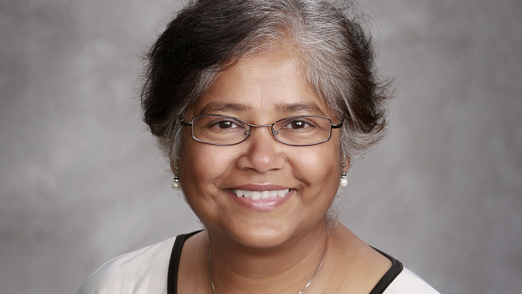
UC People: Ashfia Huq, nanoscience catalyst
Share This Article
By John German, Lawrence Berkeley National Lab
The Molecular Foundry at Lawrence Berkeley National Lab is a state-of-the-art user facility that provides expertise, methods and instrumentation for scientists to study materials at the nanoscale.
In an eight-minute audio interview — produced by Lawrence Berkeley National Lab — Molecular Foundry Director Ashfia Huq discusses the Foundry’s mission, its capabilities and some of the groundbreaking research that has been conducted there. Ashfia joined Berkeley Lab in March 2025.
Read Ashfia’s interview
Note: The content below is adapted from Berkeley Lab Chief Communications Officer John German’s interview with Ashfia (linked above).
For those who are unfamiliar with the Foundry, can you tell us what its specialty is and how it supports the nation’s science?
The Foundry is one of five knowledge-based user facilities that provide state-of-the-art, multidisciplinary expertise, methods and instrumentation in nanoscale science. User facilities are federally funded facilities that are open to external users who can come use them for free, provided the research is non-proprietary.
At the Molecular Foundry, we host over a thousand users who walk through our doors each year. They are often very early-career scientists, like graduate students and postdocs, who are enlisting the help of our scientific staff, who are experts in nanoscale science, like the synthesis and characterization of nanomaterials. We also help students, postdocs and other staff from universities, national labs and even industry who come to try to solve their research problems with the help of our scientists.
What’s different at the nanoscale? What is nanoscience and how is it different from other ways of understanding materials and chemistry?
In order for me to explain that, I’m going to go back a little bit in history.
In the early 1900s, there was a scientific revolution, mostly involving physicists, called the Quantum Science Revolution. This is when scientists realized that when you get smaller and smaller and smaller, the laws of classical physics completely fail and you start seeing new phenomena.
So, if you want to develop material with known properties, or if you are going to target a property, you need to understand materials at a very, very small atomic or molecular scale. This is essentially the field of nanoscience, which is a cross-disciplinary science that involves material science, chemistry, biology and any studies that include very, very small particles. Physicists define nano as 10 to the power minus nine. This might not make much sense to you, but if you consider the visible range that we look at things, the wavelength of light, goes from 380 nanometers to 780 nanometers.
When we’re working in scales of tens of nanometers, they’re so small that you cannot see them with light. In order for us to understand these materials and how to make or characterize them, we need special tools and methodology, which is what we develop at nanocenters.
Well, what are some of the capabilities of the foundry that people might not know about?
As I mentioned, Foundry staff are working on a very versatile set of studies which range from biotechnology to microelectronics to quantum science and quantum information systems. Because of the diversity of our research, we have a lot of different types of characterization and synthesis tools.
For example, we have robotics in the bioorganic and inorganic centers, which help us accelerate materials discovery. In the past, we used to walk into the lab and make one material per day, but that is a very slow process. Our scientists are trying to accelerate it by using modern technologies and robotics, like artificial intelligence and machine learning, which helps them look at a much larger sample to see what synthesis works and what doesn’t.
We also have to know what we have made. In order to do that, we use various techniques, like X-ray scattering, nuclear magnetic resonance and X-ray photoelectron spectroscopy — these three characterization techniques can tell us with exquisite detail how materials are forming and working in their native condition.
What are some examples of research that have benefited from the Foundry’s capabilities and expertise over the years?
Foundry staff are always pushing the boundaries of what can be done. We think, “What can we do now and what do we need to study the next generation of materials?” So, developing new tools is one of the things that the Foundry is very well known for.
One example is the transmission electron aberration-corrected microscope — which is a bit of a mouthful, so we call it TEAM. This microscope has pushed the boundary of what you can see in a material to the atomic level; you can actually see an atom, which is really, really fascinating. TEAM was developed as a Department of Energy (DOE) funded project, which involved multiple national labs and their nanocenters that also do microscopy.
Another development also came out of TEAM — we had to develop a detector for use with it because the detector technology that existed before TEAM was insufficient for atomic resolution. This new detector technology opened up a whole new field in microscopy called cryo-microscopy. This allows you to cool a sample to the point where you can look at soft and biological materials without major beam damage. Cryo-microscopy was a Nobel Prize-winning technology. Some of the earlier developments started at the Foundry are mentioned in the Nobel description of the project.
You joined Berkeley Lab in March as the director of the Foundry. What brought you here at this stage of your career, and what gets you excited about the Foundry’s research?
I have actually spent most of my scientific career at national labs. I started out as an undergraduate student walking into Brookhaven National Lab, and I was so fascinated by the big science and experiments. I got hooked. Since then, I’ve moved around in various national labs, from my Ph.D. at Brookhaven to working as staff and postdoc at other national labs.
What brought me to Berkeley Lab is its reputation for doing science. It is one of the really well-known Office of Science National Labs where fundamental research is being done. When I heard about this opportunity to lead the Molecular Foundry, I absolutely jumped on it. I am very happy to be here.